Gate-All-Around Field Effect Transistors: (GAAFETS)
Gate-All-Around
My groupmates Patrick Berne, Dan Farkash, Ryan Donnelan, and I wrote a paper on the current usages and manufacturing of Gate-All-Around Field effect transistors. This was for the class Microelectronics Manufacturing at RPI, a class in which industry professionals from the company global foundries would give insight into the semiconductor manufacturing industry. (presentation)(research paper)
Overview of Project:
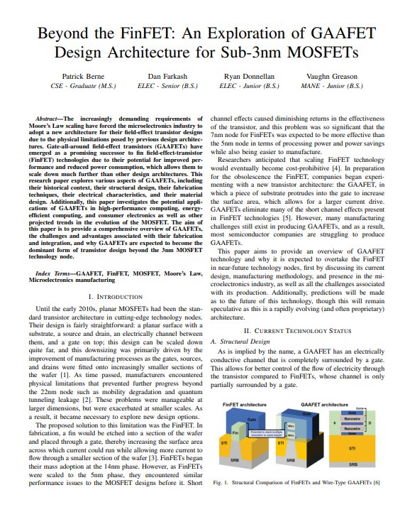
GAAFET technology is a promising successor to the FINFET technologies as short channel effects can be mitigated with the use of separate sheets/ wires protruding into the gate itself.
The major problem holding back the wide-scale fabrication of GAAFETs is the costs associated with its production.
Atomic Layer Etching is both costly and time consuming
More specialized metrology techniques such as Transmission Electron Microscopy must be used in order to create these devices.
Lateral GAAFETs
Manufacturing is easier due to similarities with FinFETs
Less scalable when compared to Vertical GAAFETs
Vertical GAAFETs
Difficult to manufacture, but much more scalable in the long term.
